Mgr. Ondřej Jašek, Ph.D.
the head of the laboratory
study of microwave plasma, carbon nanostructures and nanomaterials
Our laboratory focuses on the microwave plasma as a versatile platform for the study of plasma instabilities and the synthesis of advanced materials. In our laboratory you can also find apparatuses for preparing thin films using high-frequency discharges. The microwave and high-frequency plasma laboratory is located on the underground floor of building No.2 of the MUNI Faculty of Science campus at Kotlářská 2.
Microwave and high-frequency plasmas are simple, highly efficient, and versatile. We use them to create metal and carbon-based nanomaterials by temperature and pressure-dependent decomposition of organic precursors. Such as metal nanoparticles can further serve as a catalyst for the formation of nanotubes. Further, our laboratory uses high-temperature microwave plasmas to decompose hydrocarbons to synthesize graphene and generate hydrogen for modern power generation. We also use low-temperature, high-frequency discharge plasmas to deposit a wide range of functional layers on different types of surfaces.
Loading map…

the head of the laboratory
study of microwave plasma, carbon nanostructures and nanomaterials

study of microwave plasma and its self-organization

deposition of thin films (PECVD, PVD), characterization of mechanical properties of thin protective coatings

development of technologies for thin film preparation by PECVD and thin film analysis
Microwave plasmas can be ignited in various conditions, such as pressure, power delivery, or gaseous environments. The plasma is diffuse, filamentary, or a stream, depending on these parameters. The principle of filament excitation, its stability, the relative positions, and the behavior of individual filaments in a mixture of argon and reactive gases is one of the unresolved questions of current plasma physics, which we are investigating. We also investigate the effect of plasma temperature and electron concentration on the synthesis process of nanomaterials in the presence of organic precursors and reactive gas admixtures.


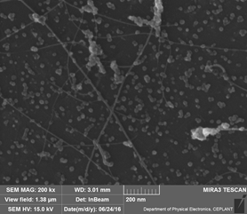
Carbon nanostructures as a material are very light and durable, have a large surface area, and good electrical and thermal conductivity. Graphene is a state-of-the-art two-dimensional carbon nanomaterial, consisting of only a single plane of carbon atoms arranged in a hexagonal graphite-like network. Carbon nanostructures can be also found in the form of fullerenes, nanocrystalline particles, nanowires, and nanotubes. Nanotubes also consist of a single atomic layer of carbon atoms, but the entire structure takes the form of single or multiple cylinders embedded in each other.
Carbon nanomaterials are used in the high-strength and tough composites for the manufacturing of tennis rackets, snowboards, cars, airplane fuselage or body of space rockets. The combination of excellent mechanical properties, chemical resistance, and large surface area allows these materials to be employed as membranes for absorbing hazardous substances, separating chemicals, or purifying water. There is also huge potential for these nanostructured materials in the energy production and large-scale production of new batteries and supercapacitors. So far, our carbon nanomaterials, especially few-layer graphene, have been used as hazardous gas sensors or composite materials for electromagnetic absorption. They have excellent electrical conductivity and exceptional resistance to oxidation at high temperatures in comparison to other carbon-based materials. At the same time, high-temperature microwave plasma is also an ideal tool for decomposing organic compounds and generating syngas or hydrogen for modern energy applications.
Nanoparticles are very small in size, diameter of 100 nm or less. We can create them in many ways and forms. Microwave plasma synthesis of nanoparticles uses high-temperature decomposition of organic precursors and subsequent formation of nanoparticles with the desired physical and chemical properties. In the past years, our laboratory has been involved, in the preparation of magnetic nanoparticles with precise phase structures, which have been tested in fields such as magnetic resonance and cell therapy, ferrofluids, or photoelectrochemical water decomposition.


There are two thin film deposition devices in our laboratory, GEC (Gaseous Electronic Cell) reactor and a reactor for large-scale thin film deposition. Both reactors are used for investigation of thin film depositions as well as plasma diagnostics.
The large-capacity reactor, called R4, is used for large-scale thin film deposition by the PECVD method. The R4 reactor was developed as a working sample in the framework of research supported by the TAČR project NCK TN01000038/17, National Centre of Competence for Materials, Advanced Technologies, Coatings and their Applications. Inside the reactor, there is a powered and a grounded electrode. The limiting pressure of the apparatus is 10-4 Pa. DC and RF sources of 13,56 MHz and 27,12 MHz can be used. The power delivered to the plasma is 0 - 600 W.
Plasma enhanced chemical vapor deposition (PECVD) is a widely used technique for thin film deposition. This method uses the energy from the plasma to split the bonds of the so-called precursor and carrier gas. These two substances then react in the reactor volume and on the reactor walls/electrodes to form a thin film. Thin films improve the surface properties of bulk materials. For example, the surface energy (wettability) and electrical, optical, and thermal properties can be enhanced while maintaining the bulk properties of the supported object. For example, protective hard diamond-like layers (DLC) are deposited on the device.