|
Physics and my research: |
Nanostructures:
Within the past several years, many
researches have devoted their attention to the investigation of
low dimensional structures in solid state physics. Due to the
small dimensions of such a structures, the size of such a systems
is comparable to nanometers, so they are called nanostructures.
The word nanostructures denotes usually objects called quantum
dots, quantum wires or quantum wells which are usually assumed as
zero dimensional (0D), one dimensional (1D) or two dimensional
(2D) objects since they can allow the electron or hole confinement
in space of the solid state. Because of this fact, such a systems
of nanostructures can reach unique optical, electronic and
magnetic properties which find huge utilization in many
practical applications and are
more and more used in optoelectronical industry in present
days. Semiconductor lasers fabricated on the basis of
nanostructures are nowadays already present in things of daily use,
such as in a common CD-player or laser pointer.
In semiconductor technology, the low dimensional structures are usually produced from III-V compounds
such a GaAs/AlAs and GaAlAs/GaAs or InP/GaP, GaAs/InAs, GaSb/InAs etc.
The first heterostructures have already been grown in 1970 based on GaAs/AlAs. These
heterostructures are nowadays contained in most of the semiconductor lasers.
Nevertheless, the production of crystals of III-V compounds is very expensive and
therefore the silicon and germanium technology is more preferable.
The first SiGe layer was grown on silicon substrate already in 1977
and the new SiGe program in semiconductor nanotechnologies has been opened.
The difference in lattice parametes of Si and Ge can be used for the formation
of self-assembled nanostructures in thin films.
The combination of silicon together with germanium offer new and chaeper perspectives
in the semiconductor nanotechnologies.
Thin films growth :
The nanostructures are mostly produced by techniques during the growth of thin films. Even the ultra
thin films are 2D nanostructures. The growth of thin films in form of multilayers (superlattices)
as a combination of repeated layers was the begining of nanotechnologies.
Earlier and nowadays, electronical devices are commonly produced using the various growth techniques with
combination of lithographical methods.
For example in present, the electron lithography is a technique approaching the resolution
to scales of order of ten nanometers. The powerful deposition techniques
which allow to grow perfect crystalline layers, pseudomorphically bound
to the substrate without dislocations, have been developed through the
years. The most developed but the time consuming method is molecular beam epitaxy (MBE).
Other epitaxial deposition techniques, also used
in nanotechnologies, are for example metal-oxide chemical vapor
deposition (MOCVD), metal-oxide vapor phase epitaxy (MOVPE),
metal-oxide molecular beam epitaxy (MOMBE), solid phase epitaxy
(SPE) and others.
The advantage of the lithography
is a good control of size and homogeneity of the structure, on the
other side there are also many disadvantages. The size of the
objects is limited by the wavelength of the used radiation during
the lithography and the etching process of the quantum dots or
wires during developing usually incorporates defects on the sides
of the objects which deteriorates the optoelectronical properties of the
structures. The another disadvantage of the lithographical methods
is that they are very slow (repeated process of the layer
deposition and photoresist removal) and thus economically
disadvantageous.
Next to the lithographical methods, also the techniques of self
assembled growth directly during epitaxy can be used for the production
of nanostructures. These are relatively new methods of nanostructure
production with respect to semiconductor history, although the
principles come originally from the first half of the 20th century,
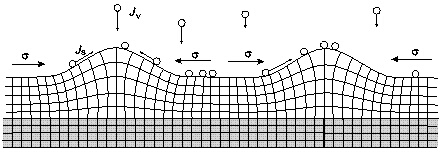
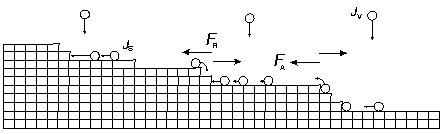
The techniques are mainly based on the Stranski-Krastanow (SK)
growth mechanism and step bunching mechanism.
The quantum dots or wires are produced directly during the layer
deposition. Since the layer deposited on the substrate is elastically
strained, the growing interface results in surface modulations
laterally ordered, after the deposition of several monolayers (ML).
With this procedure, a quantum structures can be created where
their productionn is economically much more preferable.
Unfortunately, the formation of such a patterns is conditioned by various parameters,
determined above all by the deposited material and by its structure,
sample temperature and other ambient conditions. The
growth control is still method of experiment. The fluctuations of the structural
parameters of the grown nanoobjects decrease optical and
electronic properties.
Scanning probe microscopy:
The structural characteristics of nanoobjects can be studied by
various experimental methods. The most frequently used methods are
atomic force microscopy (AFM), scanning tunneling microscopy (STM), scanning electron microscopy (SEM),
transmission electron microscopy (TEM), rapid high energy electron
diffraction (RHEED) and finaly also x-ray scattering (XRS) methods.
The advantage of methods such as AFM, STM, SEM, TEM is in their easily
interpretable data since they produce real space images of the material
structure and thus they give more clear idea about the investigated structure.
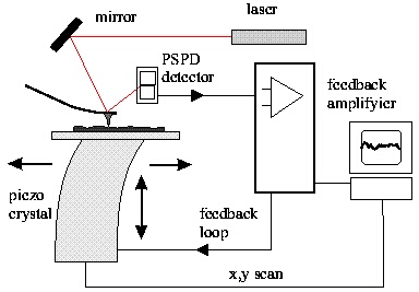
AFM is one of the method from the family of
instruments used for investigation of surface properties of
materials from the atomic to micron level; among the other SPM
methods, such as scanning tunnelling microscopy (STM), magnetic
force microscopy (MFM), lateral force microscopy (LFM). The AFM
is based on the scanning of the surface with a sharp tip, a couple
of microns long and often less than 10 nm wide in diameter, and
also on measuring the force interaction between the tip and the
surface. The topographic image is generated from the distribution of
the tip-surface force fluctuations along the surface. This
interatomic force associated with AFM is called van der Waals force.
Generally, we can distinguish two basic scanning modes how to record
a topographical image. The most currently used is the mode of
constant force. By means of the feedback loop, the distance
tip-sample is held constant
and the vertical position of the whole sample is changed.
The image is generated from the vertical sample positoin and the vertical
profile of the sample surface is recorded.
The second scanning mode is constant height mode. In this
case, the spatial variation the tip is used for
direct generation of the topographic data which generates the image
of the surface. During the scan, the vertical position of the sample is
fixed and the tip position is detected by the laser. This
mode is often used for taking atomic-scale images of very flat
surfaces since the cantilever deflection must be small.
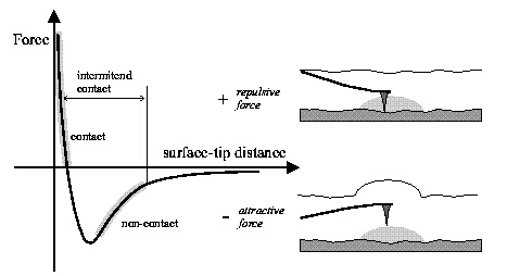
Depending on the value of van der Waals force we distiquish the regimes in AFM:
Contact regime - the interaction between the
sample and tip is repulsive. The tip makes soft physical
contact with a sample.
Non-contact regime - the interaction between the
sample and tip is attractive. Since the force between the tip and the surface is very low, it is
more difficult to measure the force.
The disadvantage of the AFM measurements is that they are only local sensitive.
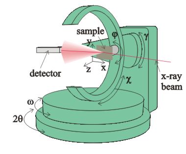
X-ray scattering methods (XRR, XRD, GID, GISAXS):
To the methods, sensitive to the large area of the sample in average, the x-ray scattering techniques belong since they are locally
sensitive only in reciprocal space and thus the information
from the measurement is averaged over the whole irradiated sample area.
On the other hand, the disadvantage of the scattering experiments is that the proper
theoretical model must be found and applied to the measured data to get
a realistic imagination about the sample structure.